
Integrating 2D materials for on-chip photonics
KNOXVILLE, TN, October 05, 2023 /24-7PressRelease/ — Interests surrounding the development of on-chip nonlinear optical devices have grown consistently in the past decades due to their tremendous applications. Developing efficient on-chip nonlinear optical devices for these applications is needed to improve the existing photonic approaches. The combination of well-known photonic chip design platforms and different two-dimensional layered materials has opened the road for more versatile and efficient structures and devices, which has the great potential to unlock numerous new possibilities.
Recently, the introduction of nonlinear optical functions in integrated optics has sparked significant enthusiasm. Demonstrations have shown the potential for integrated photonic platforms. Furthermore, large-scale manufacturing capability and affordability have motivated the development of fully integrated, nonlinear optical devices, aiming at various applications, such as all on-chip spectroscopy, on-chip quantum computations and communications, efficient multiplexing for data communications, on-chip metrology, bio-sensing, or LIDARs.
In a new paper published in Light: Advanced Manufacturing, a team of scientists led by Professors Vincent Pelgrin and Zhipei Sun have reviewed the range of hybrid photonic integration structures.
Integrating these different active functions in silicon photonics has also attracted much attention. The possible compatibility with CMOS processes and the overall low cost of the platform indeed make it very attractive to the industry, with devices directly suitable for dense optical circuit fabrication. These deep integration capabilities make the Si-compatible platform an interesting testbed for the transposition. Silicon photonics presents some impediments when considering the exploitation of nonlinear optical processes. These are primarily the weak nonlinear responses of the most common materials compatible with its clean room processes or to the presence of free carriers.
Si is highly nonlinear in the C-band range but suffers from Two Photons Absorption (TPA) due to its low bandgap. Unfortunately, most classical materials compatible with silicon integration lack strength in terms of optical nonlinearities. The stochiometric SiN nonlinear refractive index (n2) is almost two orders of magnitude lower than Si. The stochiometric SiN nonlinear refractive index (n2) is nearly two orders of magnitude lower than Si.
Impressive demonstrations have been presented using various silicon-based materials to generate integrated optical functions. These include supercontinuum sources, frequency combs, and photon pair sources through spontaneous four-wave mixing. In some fields, the communities have pushed for more efficient devices showing high performance with low power consumption. Annealed SiN waveguides with loss levels of a few dB/m have been demonstrated, but the needed pump power was still large. Long waveguides were required to achieve sufficient nonlinear processes, thus making optical functions demanding for fully integrated devices.
Alternatively, materials such as Si-rich waveguides or using p-i-n junctions to engineer carrier density have shown some promising results. However, there are some drawbacks. Si-rich waveguides still present TPA. At the same time, using multiple p-i-n junctions adds another layer of complexity to devices and circuits. Hence, the need for solutions to this limitation is still strong.
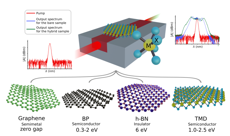
Another approach is to introduce highly nonlinear materials to the on-chip platform to take advantage of the highly effective properties of these materials. This approach boosts their nonlinear performance via the integration strategy. Several materials have been tested throughout the past decade. Chalcogenides are a popular alternative to Si-based materials. In the quest to identify disrupting nonlinear optical materials, two-dimensional (2D) layered materials have been identified as extremely promising. These materials have third-order susceptibility up to two orders of magnitude higher than Si.
The most widely known material in this category is graphene. Still, other 2D materials such as Transition Metal Dichalcogenide (TMDs). The MX2 crystals are where M stands for a metal atom and X for a chalcogen). BP is also receiving increasing attention. The principle behind hybrid integration consists in incorporating high-performance 2D materials into the existing integration platforms, thus increasing the overall effective nonlinear performance of the waveguides.
Several challenges arise from the hybrid integration approach, as 2D materials are still not fully understood. The impact of their addition to integrated structures needs to be handled carefully. The review presents recent progress in the field and the team’s perspectives. They briefly introduced the theoretical background of the hybrid integration of 2D materials for the different integrated optics platforms. The aim is to describe key steps, from the modeling and the design to the characterization steps. This will hopefully serve as a guideline for future works on the related fields, thus solving one of the obstacles met with integrated nonlinear photonics.
References
Funding
This work was supported by Paris Saclay University within the Centre for Nanoscience and Nanotechnology (C2N) in France and Aalto University in Finland, the Academy of Finland, the Academy of Finland Flagship Programme, the EU, and ERC.
Contact
Vincent Pelgrin
QTF Centre of Excellence, Department of Electronics and Nanoengineering, Aalto University, P.O. Box 13500, FI-00076 Aalto, Finland, [email protected]
DOI
10.37188/lam.2023.014
Original Url
https://light-am.com/article/doi/10.37188/lam.2023.014
About Light: Advanced Manufacturing
Light: Advanced Manufacturing (LAM) is a new, highly selective, open-access, and free of charge international sister journal of the Nature Journal Light: Science & Applications. The journal aims to publish innovative research in all modern areas of preferred light-based manufacturing, including fundamental and applied research and industrial innovations.
Chuanlink Innovations, where revolutionary ideas meet their true potential. Our name, rooted in the essence of transmission and connection, reflects our commitment to fostering innovation and facilitating the journey of ideas from inception to realization.
Related Link:
http://chuanlink-innovations.com
—
For the original version of this press release, please visit 24-7PressRelease.com here